

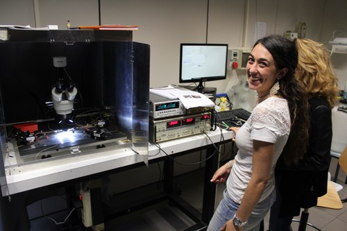
We are experts in low signal AC and DC electrical characterizations. Our laboratory is equipped with a probestation and all the necessary electronic instrumentation to characterize nano- and microelectronic devices with signal levels down to the femto-Amper and nano-Volt range. This allows us to determine characteristic electrical parameters such as trasport mobilities, interfacial capacitances, threshold voltages and many more with high precision.
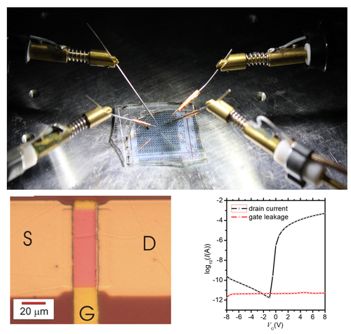
Thin film transistors (TFT) are the basic microelectronic component of integrated circuits. For us physicists they are also a versatile test device to characterize transport properties in novel semiconducting materials. The field effect is exploited in TFT to introduce a well quantified amount of free charge cariers. The DC current across the semiconducting channel then provides information about how fast these carriers move and other material specific parameters. Our electronic instrumentation permits the precise measurement of the related electronic signals. The figure to the left features as an example the characterization of an amorphous oxide semiconductor based TFT fabricated at the University of Lissbon in Protugal. Micromanipulator probes are used to connect the TFT electrically to our measurement instrumentation. The DC current measurements then reveal optimal TFT behaviour with a steep transition between on/off range, low off- currents in the range of a few pico-amperes and a high mobility of 19 cm2/Vs.
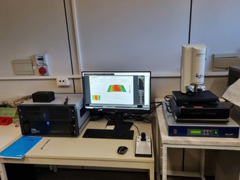
SmartWLI - 3D Optical Profilometer
3D optical surface profilometer for in-line and mobile use, designed for high-performance applications requiring short cycle times. It features a piezo motor for sub-nanometric resolution and an optional precision mechanical axis to extend the Z-range. It enables real time 3D image analysis. Optimized for the following applications: Surface Science, Optoelectronic Property Analysis, Polymer and Semiconductor Material Characterization, 3D Surface Roughness Measurement, and Surface Coating Characterization. Equipped with:four objective Nikon 5x, 10x, 20x, 50x; an active table for vibration noise reduction; image analysis software MountainsMap® Imaging Topography V9.
Funded by Next Generation EU - Project iENTRANCE@ENL - Infrastructure for energy transition and circular economy@EuroNanoLab
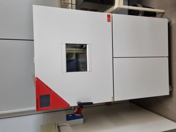
Climatic Chamber - Binder MFKT 115
Climatic Chamber enables both static and dynamic variations with climate changes ranging from -70°C to 180°C, with extensive reserves and, in particular, rapid cooling at a constant rate (5 K/min). It is equipped with an electronic device for humidification and dehumidification (10-98%RH), featuring a capacitive humidity sensor and pressurized steam. It also includes an Ethernet network connection for use with the APT-COM™ control software, supporting GLP/GMP validations in accordance with 21 CFR Part 11 guidelines.
Funded by Next Generation EU - Project iENTRANCE@ENL - Infrastructure for energy transition and circular economy@EuroNanoLab
Cramer, Tobias; Sacchetti, Allegra; Lobato, Maria Teresa; Barquinha, Pedro; Fischer, Vincent; Benwadih, Mohamed; Bablet, Jacqueline; Fortunato, Elvira; Martins, Rodrigo; Fraboni, Beatrice, Radiation-Tolerant Flexible Large-Area Electronics Based on Oxide Semiconductors, «ADVANCED ELECTRONIC MATERIALS», 2016, 2, pp. 1 - 8
T. Cramer; A. Kyndiah; A. Kloes; M. Murgia; B. Fraboni; F. Biscarini, Charge density increase in submonolayer organic field-effect transistors, «PHYSICAL REVIEW. B, CONDENSED MATTER AND MATERIALS PHYSICS», 2015, 91, pp. 1 - 7
The document explains important concepts about our probestation.